

Solution Center
‌Xinchangyuan Direct Fluid Writing Solution for the Miniaturization Era
‌ONEWTECH‌ leads the new paradigm of chip manufacturing

Solution CenterSolution Center

‌Mass Production in 2026 Unlocks a New Era of Miniaturized Manufacturing‌

The semiconductor industry is undergoing a paradigm shift from planar scaling to 3D stacking, with packaging process precision requirements leaping to the sub-micron level. ‌precisely targets the technological vacuum zone, establishing its strategic leadership in the fluid direct-write field in the miniaturization era.

2023
Global R&D and Sales Network Construction
Founded in Suzhou, it has built an R&D network covering Shanghai, Sendai and Hong Kong, China, bringing together top experts in fluid control.
2024
INK JET R&D Breakthrough
Successfully developed a new generation of direct writing printing technology, breaking the bottleneck of traditional piezoelectric printheads in micro-droplet control.
2025
Engineering Prototype Test Succeeded
The world's first engineering prototype has verified its excellent performance in smaller-size chips and higher-precision operations.
2026.10
Mass Production Equipment Put into Testing
The first mass production equipment has been put into the production line, and successfully completed the Under Fill process test for small-size chips.
01
Address the market supply-demand gap
Meet the expansion demands of advanced packaging, and eliminate the inertial dependence on traditional equipment in the era of large-size chips.
02
‌Customization for Emerging Fields
Provide customized direct writing capabilities for Mini LED, Quantum Conversion, MEMS and L-COS‌.
03
Process Mass Production Certainty
Provide full-process support from process validation to mass production, and break the situation of relying on imported equipment that is difficult to adapt to new materials.

5pl Ultimate Precision & 10kHz Spraying Revolution‌

Minimum Dispensing Volume
5pl
‌Ultra-high Jetting Frequency
20,000cycles per second
  • Accuracy exceeds industry standards

    Far exceeding the industry 7pl standard, the adaptability to high-viscosity adhesives has achieved a qualitative leap.

    Complete hundreds of millions of precise depositions in an extremely short time to break through the production capacity bottleneck.

  • ‌Multi-jet Parallel Architecture

    Innovatively adopt a multi-jet parallel architecture on a single unit.

    Break through the efficiency ceiling of traditional single-jet systems and enable large-area simultaneous direct writing.
  • ‌Mini LED Mass Transfer‌
    Large-area simultaneous direct writing, with the production tact time reduced by more than 40%.
  • ‌2.5D / 3D Advanced Packagin
    Non-contact jetting, with the error controlled within ±0.01mm.
  • Biomedicine and MEMS
    Waveform optimization maintains molecular integrity and prevents material denaturation.
  • Higher-Performance Adhesive Jetting
    Supports brand-new UV adhesive jetting, enabling direct processing of high-end underfill materials.

Japan-based Collaborative Verification of Underfill Process‌

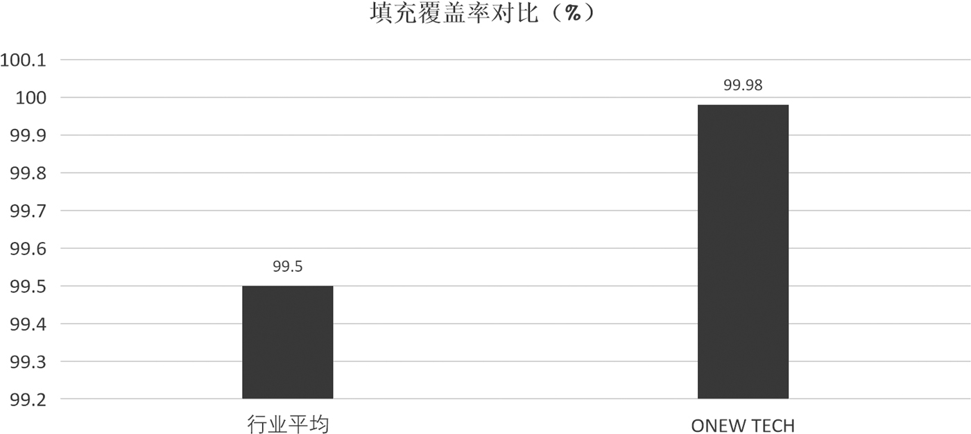
In the field of advanced packaging, the stability of the underfill process directly determines the reliability of chips under thermal cycling and mechanical stress.

  • 99.98%
    Filling Coverage Rate
  • <0.01%
    ‌Bubble Residual Rate
  • 0.07mm
    ‌Minimum Coating Pitch / Gap
  • Japan Collaboration and Extreme Testing
    We have established deep partnerships with multiple top-tier adhesive manufacturers in Japan. Through 18 months of extreme pressure testing conducted at the Sendai R&D Center, we have successfully overcome the long-standing challenges of ‌adhesive bleed-out‌ and ‌void formation‌ under high-density arrays of small-sized chips.
  • ‌Breakthrough in Mini LED COB Packaging
    Leveraging its 5pL precise glue control capability, the system enables accurate deposition of adhesive within the capillary action zone at the edge of the chip, eliminating the risks of adhesive bridging, optical crosstalk or electrical short circuits caused by traditional dispensing under ultra-high-density layouts.
  • 2.5D / HBM Stacking Solution
    For silicon interposer and HBM stacking structures, the exclusive direct-write process formulation effectively solves the stress concentration problem caused by multi-layer stacking, and significantly improves the overall mechanical strength and heat dissipation efficiency of the module.
  • Access Pass and Total Solution
    We deliver an integrated "Equipment + Material + Process" total solution, whose relevant data has been incorporated into the review systems of multiple leading wafer fabs, marking the first time that domestic equipment has obtained the ‌Access Pass‌ in the world's top-tier material systems.